Using 'Scotch tape' and laser beams, researchers craft new material that could improve LED screens

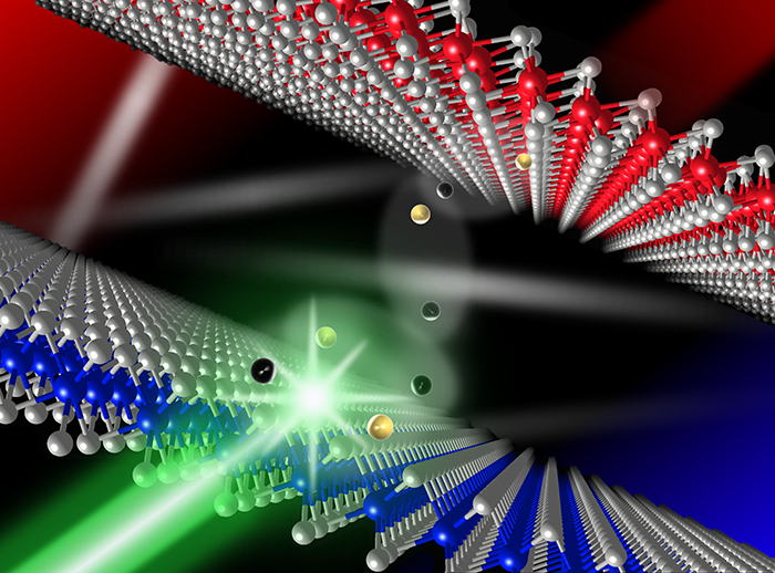
LAWRENCE — A cover story appearing in the peer-reviewed journal Nanoscale Horizons reports a new bilayer material, with each layer measuring less than one nanometer in thickness, that someday could lead to more efficient and versatile light emission.
Researchers working at the Ultrafast Laser Lab at the University of Kansas successfully created the material by combining atomically thin layers of molybdenum disulfide and rhenium disulfide.
“Both absorb light very well as semiconductors, and they’re both very flexible can be stretched or compressed,” said Hui Zhao, associate professor of physics and astronomy at KU, who co-authored the paper. “The goal of this whole direction of research is to produce light-emitting devices, such as LEDs that are ultrathin — just a few nanometers thick — and flexible enough that you can bend it. We showed through this bilayer material, it can be achieved.”
To explain the breakthrough, Zhao likens the behavior of electrons in the new material to a classroom.
“One can think of a material as a classroom full of students — which are the electrons — one on each seat,” he said. “Sitting on a seat, a student — or electron — can’t move freely to conduct electricity. Light can provide enough energy to stand up some of the students, who can now move freely and, as electrons, to conduct electricity. This process is the foundation for photovoltaic devices, where the energy of sunlight is captured and converted to electricity.”
The KU researcher said that emission of light involves the inverse process, in which a standing electron sits down in a seat, releasing its kinetic energy in the form of light.
“To make a good material for light emission devices, one needs not only the electrons that carry energy, but also the ‘seats’ — called holes — for the electrons to sit down,” he said.
Previous studies by several groups, including Zhao’s, have produced various bilayer materials by stacking different types of atomic sheets. However, in these materials, the electrons and the “seats” exist in different atomic layers.
“Because electrons cannot easily find seats, light emission efficiency of these bilayer materials is very low – more than 100 times lower than in one atomic layer,” he said.
But in the new material announced by Zhao and his co-authors, “All the electrons and their seats will be in their original layer, instead of separate. The light emission will be a lot stronger.”
Zhao and fellow researchers Matthew Bellus, Samuel Lane, Frank Ceballos and Qiannan Cui, all KU physics graduate students, and Ming Li and Xiao Cheng Zeng of the University of Nebraska-Lincoln created the new material using the same low-tech “Scotch tape” method pioneered in creating graphene, the single-atomic-layer material that won its creators the Nobel Prize for physics in 2010.
“There’s a trick,” Zhao said. “You use Scotch tape to peel off a layer from the crystal and then you fold the tape a few times, so when you push the tape against a substrate and quickly peel it off, some of the material will be left on the substrate. Under a microscope, single-atom layer sections will have a different color because of their thickness — very much like a thin film of oil on water.”
The researchers at KU’s Ultrafast Laser Lab, led by Bellus, the first author of the paper, then accomplished the most challenging step: stacking the MoS2 layer on top of ReS2, with a precision better than one micrometer. The atomically thin sheets were connected by the so-called van der Waals force, the same force which allows a gecko to scale a smooth window pane. “The van der Waals force isn’t very sensitive to the atomic arrangement,” said Zhao. “So, one can use these atomic sheets to form multilayer materials, in a fashion like atomic Legos.”
After the samples were made, team members used ultrafast lasers to observe motion of electrons and seats between the two atomic layers, and they saw clear evidence that both electrons and the seats can move from MoS2 to ReS2, but not along the opposite direction.
In doing so, the team confirmed theoretical calculations performed by Li and Zeng, who previously had analyzed related properties of about a dozen atomic sheets, and predicted that bilayers formed by MoS2 and ReS2 would have promise as the basis for LED technology.
According to Zhao, the ultimate goal is to develop a method that allows precise control of the location of electrons and seats among different atomic layers so that the electronic and optical properties of the material can be controlled and optimized.
“We’d someday like to see LEDs that are thinner, more energy efficient and bendable,” he said. “Think about a computer or phone screen if you could fold it a few times or and put it in your pocket.”
The National Science Foundation supported this research.